
PCB SMT assembly chip refers to the abbreviation of process flow based on PCB. What is its basic process and what are its processes? Today, I will talk about the basic technology and process of PCB SMT assembly.
1.
The basic technology of PCB SMT assembly is as follows:
Solder paste printing → parts mounting → reflow soldering → AOI optical detection → maintenance → plate splitting.
Electronic products pursue miniaturization, and the previously used perforated plug-in components can no longer be reduced. The functions of electronic products are more complete, and the integrated circuit (IC) used has no perforated components, especially the large-scale and high integrated IC, so surface mount components have to be used. With mass production and automatic production, manufacturers should produce high-quality products with low cost and high output to meet the needs of customers and enhance market competitiveness. The development of electronic components, the development of integrated circuits (IC) and the diversified application of semiconductor materials. The revolution of Electronic Science and technology is imperative to pursue the international trend. It can be imagined that the development of PCB SMT assembly surface assembly technology and process is also inevitable when the production process of Intel, AMD and other international manufacturers of CPU and image processing devices has advanced to more than 20 nanometre.
Advantages of PCB SMT assembly chip processing:
With high assembly density, small volume and light weight of electronic products, the volume and weight of PCB SMT assembly components are only about 1 / 10 of that of traditional plug-in components. Generally, PCB SMT assembly can reduce the volume of electronic products by 40% - 60% and the weight by 60% - 80%. It has high reliability, strong anti vibration ability, low defect rate of solder joint, good high frequency characteristics, and reduces electromagnetic and radio frequency interference. It is easy to realize automation and improve production efficiency. Reduce costs by 30% - 50%. Save materials, energy, equipment, manpower, time, etc.
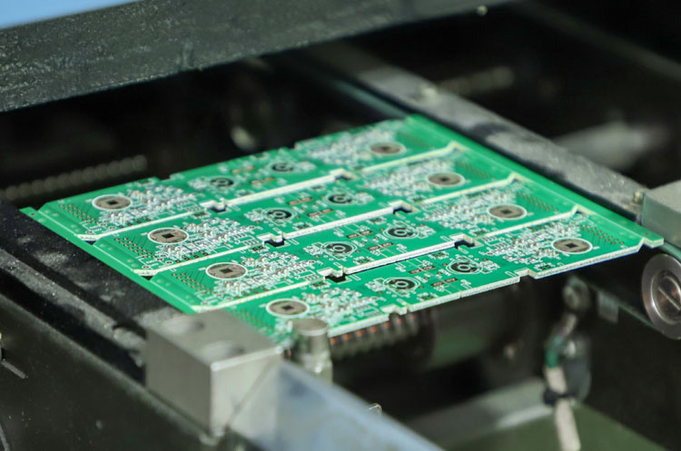
It is because of the complexity of PCB SMT assembly chip processing process, so there are many PCB SMT assembly chip processing factories, specializing in PCB SMT assembly chip processing. In Shenzhen, thanks to the vigorous development of the electronic industry, PCB SMT assembly chip processing has made an industry prosperous.
2. PCB SMT assembly patch process
The basic elements of PCB SMT assembly include: silk printing (or dispensing), mounting (curing), reflow welding, cleaning, testing, repair
1) Screen printing: it is used to seal solder paste or adhesive to PCB pad, and prepare for welding of components. The equipment used is screen printing machine (screen printing machine), which is located at the front end of PCB SMT assembly production line.
2) Dispensing: it drops glue onto the fixed position of PCB board, and its main function is to fix components to PCB board. The equipment used is a dispensing machine, located at the front end of PCB SMT assembly production line or behind the detection equipment.
3) Mounting: its function is to accurately install the surface assembly components to the fixed position of PCB. The equipment used is a chip machine, located in the PCB SMT assembly production line behind the screen printing machine.
4) Curing: the function is to melt the adhesive, so that the surface assembly components and PCB board are firmly bonded together. The equipment used is curing furnace, which is located behind the PCB SMT assembly production line.
5) Reflow welding: the function is to melt the solder paste, so that the surface assembly components and PCB board are firmly bonded together. The equipment used is reflow welding furnace, which is located behind the PCB SMT assembly production line.
6) Cleaning: the function is to remove the harmful welding residues such as flux on the assembled PCB board. The equipment used is a cleaning machine, and its position can be fixed, online or not.
7) Inspection: its function is to inspect the welding quality and assembly quality of the assembled PCB. The equipment used includes magnifying glass, microscope, on-line tester (ICT), flying needle tester, automatic optical detection (AOI), X-ray detection system, function tester, etc. The location can be arranged in the right place of the production line according to the needs of the detection.
8) Repair: its function is to rework PCB board which detects fault. The tools used are soldering iron, repair workstation, etc. Configuration is at any position in the production line.
Above is the detailed introduction of the "PCB SMT assembly patch basic process and process". If you have other problems, please keep your attention on us!
Hello, welcome to visit our official website!
+86 13502814037 (What's up)sales@topscompcbassembly.com
Turnkey Pcba Assembly & Contract Electronic OEM Manufacturing Provider

