
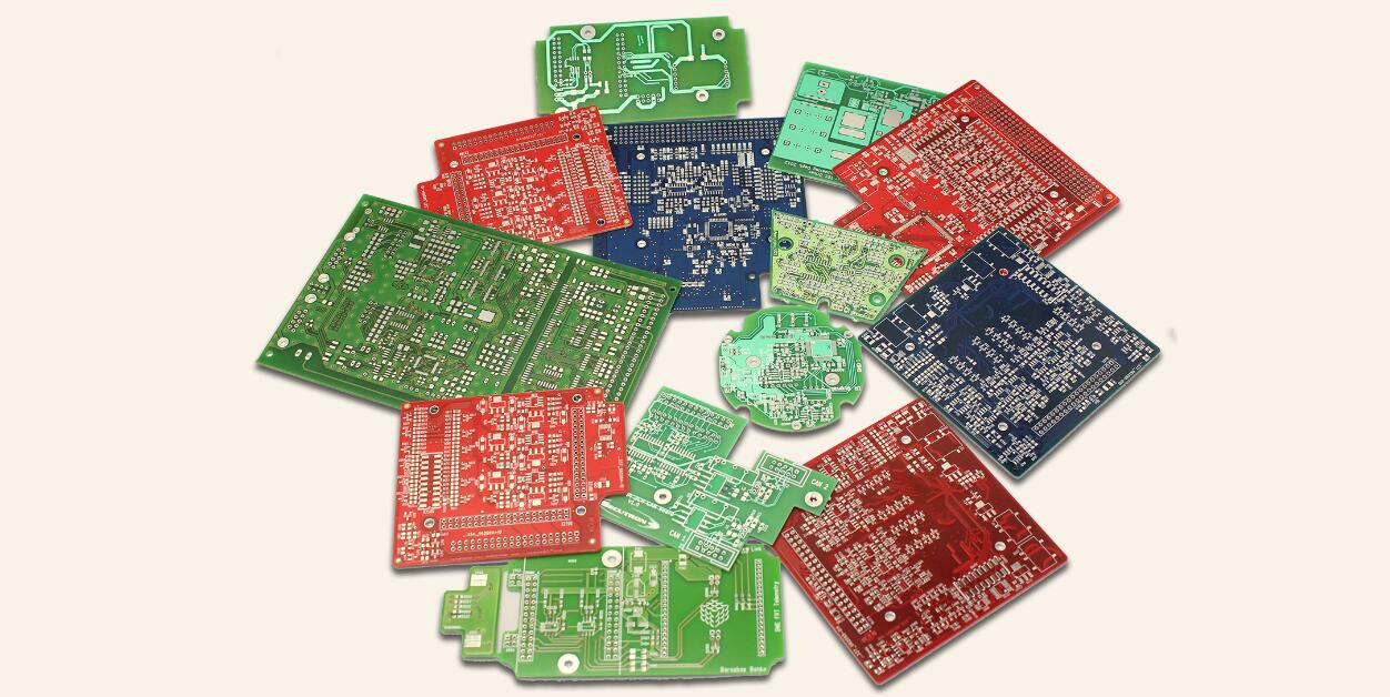
Pcb board design specifications standards (Topscom Internal File)
1.. 1 PCB (Print circuit Board): printed circuit board.
- 2 schematic diagram: a circuit schematic diagram drawn with a schematic design tool to express the connection relationship between various devices in a hardware circuit.
1.. 4 layout: the process of placing components on the board in accordance with the design requirements in the PCB design process.
1.. 5 Simulation: with the support of IBIS MODEL or SPICE MODEL of the device, using EDA design tool to.
The layout and routing effect of PCB are simulated and analyzed, so that the EMC problems, timing problems and signal integrity problems in the design are found before the physical implementation of the veneer, and the appropriate solutions are found.
Purpose.
a. This specification summarizes the PCB design process and design principles of our company, and the main purpose is to provide PCB designers with rules and conventions that must be followed.
b. Improve PCB design quality and design efficiency.
Improve the productivity, testability and maintainability of PCB.
ii. Design task acceptance.
A. PCB design application process.
When the hardware project personnel need to carry out the PCB design, they must submit the board application in the PCB Design Board Application form, and after the approval of the project manager and the planning department, the process status will be approved by the designated PCB design department. At this time, the hardware project personnel shall prepare the following information:
1 reviewed, completely correct schematics, including paper documents and electronic parts;
2 formal BOM; with MRPII component coding.
3PCB structure diagram, should indicate the external dimensions, mounting hole size and positioning dimensions, connector positioning dimensions, no wiring area and other related dimensions;
(4) for new devices, that is, devices without MRPII coding, package data need to be provided.
The PCB design can be started only after the above information has been approved by the designated PCB design department and the PCB designer has been designated.
b. Understand design requirements and make design plan.
1. Read the schematic diagram carefully and understand the working conditions of the circuit. Such as the working frequency of the analog circuit, the working speed of the digital circuit and other elements related to the wiring requirements. Understand the basic functions of the circuit, the role in the system and other related issues. the article is posted by Dr.liu surong,director of Topscom pcb design layout R&D department,china Topscom provide high difficulty density & printed circuit boards PCB design & layout, mass manufacturing & fabrication,pcba boards assembly.
2. On the basis of full communication with the schematic designer, confirm the key networks on the board, such as power supply, clock, high-speed bus, etc., to understand their wiring requirements. Understand the high-speed devices on the board and their wiring requirements.
3. According to the requirements of "hardware schematic Design Specification", the schematic is reviewed.
4. For the places in the schematic that do not meet the hardware schematic design specifications, we should clearly point out and actively assist the schematic designer to modify.
5. On the basis of communicating with the schematic designer, the PCB design plan of the veneer is worked out, and the design record table is filled in. The plan should include the time requirements of the key checkpoints in the design process, such as schematic input, layout completion, wiring completion, signal integrity analysis, light drawing completion and so on. The design plan shall be signed and approved by both the PCB designer and the schematic designer.
6. If necessary, the design plan shall be approved by the superior.
iii. Design process.
a. Create a network table.
1. The network table is the interface file between the schematic diagram and PCB. PCB designers should choose the correct network table format and create a network table that meets the requirements according to the characteristics of the schematic diagram and PCB design tools.
two。 In the process of creating the network table, we should actively assist the schematic designer to eliminate errors according to the characteristics of the schematic design tool. Ensure the correctness and integrity of the network table. the article is posted by Dr.liu surong,director of Topscom pcb design layout R&D department,china Topscom provide high difficulty density & printed circuit boards PCB design & layout, mass manufacturing & fabrication,pcba boards assembly.
3. Determine the package (PCB FOOTPRINT). Of the device.
4. Create a PCB board.
Create the PCB design file according to the veneer structure diagram or the corresponding standard board frame, and pay attention to the correct selection of the location of the veneer coordinate origin and the setting principle of the origin:
1 the intersection of the extension line on the left and the lower side of the veneer.
2 the first pad in the lower left corner of the veneer.
Fillet around the plate and frame, chamfer radius 5mm. Refer to the structural design requirements for special cases.
b. Overall Arrangement.
1. Set the size of the plate and frame according to the structure drawing, and arrange the installation holes, connectors and other devices that need to be positioned according to the structural elements.
And immovable properties are given to these devices. Dimensions are carried out according to the requirements of the process design specification.
2. The prohibited wiring area and the prohibited layout area of the printed board are set up according to the structure diagram and the clamping edge required for production and processing. According to the special requirements of some components, no wiring area is set.
3. The machining process is selected by considering the performance of PCB and the efficiency of machining.
The optimal order of processing technology is as follows: single-sided assembly of component surface-component surface mounting, plug-in mixed assembly (component surface plug welding surface mounting once wave forming)-double-sided placement-component surface placement mixed assembly, welding surface mounting.
4. Basic principles of layout operation.
a. Follow the layout principle of "big before small, difficult before easy", that is, important unit circuits and core components should be given priority.
b. The layout should refer to the principle block diagram and arrange the main components according to the main signal flow law of the veneer.
c. The layout should meet the following requirements as far as possible: the total connection is as short as possible, and the key signal line is the shortest; high voltage and high current signals are completely separated from low current and low voltage weak signals; analog signals are separated from digital signals; high frequency signals are separated from low frequency signals; high frequency components should be fully spaced. the article is posted by Dr.liu surong,director of Topscom pcb design layout R&D department,china Topscom provide high difficulty density & printed circuit boards PCB design & layout, mass manufacturing & fabrication,pcba boards assembly.
d. In the part of the circuit with the same structure, the "symmetrical" standard layout is adopted as far as possible.
e. Optimize the layout according to the standards of uniform distribution, balanced center of gravity and beautiful layout;
f. Device layout grid setting, in general IC device layout, the grid should be 50 mil, 100 mil, small surface mount devices, such as surface mount components layout, the grid setting should not be less than 25mil.
g. If there are special layout requirements, it should be determined after communication between both parties.
5. The same type of plug-in components should be placed in one direction in the X or Y direction. The same type of polar discrete components should also strive to be consistent in the X or Y direction, so as to facilitate production and inspection.
6. The heating elements should be uniformly distributed to facilitate the heat dissipation of the veneer and the whole machine, and the temperature sensitive devices other than the temperature detection elements should be far away from the components with high heat generation.
7. The arrangement of components should be convenient for debugging and maintenance, that is, large components can not be placed around small components, elements that need to be debugged, and there should be enough space around the device.
8. For the veneer produced by wave soldering process, the fastener installation hole and positioning hole should be non-metallic hole. When the installation hole needs to be grounded, it should be connected with the ground plane by distributing grounding holes.
9. When the mounting components of the welding surface are produced by wave soldering process, the axial direction of the resistance and capacity should be perpendicular to the transmission direction of wave soldering, the resistance row and SOP (PIN spacing is greater than or equal to 1.27mm) the axial direction of components is parallel to the transmission direction; active components such as IC, SOJ, PLCC, QFP, etc., whose PIN spacing is less than 1.27mm (50mil), avoid wave soldering.
10. Distance between BGA and adjacent components > 5mm. The distance between other patch elements is more than 0.7mm; the distance between the outside of the pad of the mounting element and the outside of the adjacent plug-in components is more than 2mm; there can be no plug-in elements and devices in the 5mm around the PCB, crimping connector of the crimped parts, and there can be no placement elements and devices in the 5mm around the welding surface.
11. The layout of the IC decoupling capacitor should be as close to the power pin of the IC as possible and make the circuit between the power supply and the ground as short as possible.
twelve。 In the layout of components, appropriate consideration should be given to putting the devices using the same power supply together as far as possible, so as to facilitate the separation of power supplies in the future. the article is posted by Dr.liu surong,director of Topscom pcb design layout R&D department,china Topscom provide high difficulty density & printed circuit boards PCB design & layout, mass manufacturing & fabrication,pcba boards assembly.
13. The layout of resistance-capacitance devices for impedance matching should be arranged reasonably according to their properties.
The layout of the series matching resistor should be close to the driving end of the signal, and the distance generally does not exceed 500mil.
The layout of matching resistors and capacitors must distinguish between the source and the terminal of the signal, and the terminal matching with multiple loads must be matched at the farthest end of the signal.
14. After the layout is completed, the assembly drawing is printed for the schematic designer to check the correctness of the device package, and confirm the signal correspondence of the veneer, backplane and connector, and then start wiring after confirmation.
c. Set routing constraints.
1. Report Design Parameter 8.
After the layout is basically determined, the statistical function of PCB design tool is used to report the basic parameters such as network number, network density, average pin density and so on, in order to determine the number of signal wiring layers needed.
The number of signal layers can be determined by referring to the following empirical data.
1Pin density.
2 signal layers.
3 number of plates.
Note: PIN density is defined as: plate area (square inch) / (total number of pins on board / 14).
The specific determination of wiring layers should also take into account the reliability requirements of the veneer, the working speed of the signal, manufacturing cost and delivery time and other factors.
1. Wiring layer Setting.
In the design of high-speed digital circuit, the power supply and the stratum should be close together as far as possible, and no wiring should be arranged in the middle. All wiring layers are as close to a plane layer as possible, and the preferred ground plane is the wiring isolation layer.
In order to reduce the electromagnetic interference of interlayer signals, the direction of the signal line of the adjacent wiring layer should be vertical.
Two impedance control layers can be designed according to the need, and if more impedance control layers are needed, you need to negotiate with the PCB manufacturer. The impedance control layer should be clearly marked as required. The network wiring with impedance control requirements on the veneer is distributed on the impedance control layer.
2. Settings for line width and line spacing.
Factors to be considered in the setting of line width and line spacing.
a. The density of the veneer. The higher the density of the plate, the greater the tendency to use thinner lineweights and narrower gaps.
b. The current strength of the signal. When the average current of the signal is large, the current that can be carried by the wiring width should be considered, and the linewidth can be referred to the following data:
The relationship between copper foil thickness, wire width and current in PCB design the ampacity of copper foil with different thickness and width is shown in the following table:
Copper thickness 35um copper thickness 50um copper thickness 70um copper skin 10 ℃ note:
i. When using copper skin as a wire to pass through a large current, the ampacity of the width of the copper foil should be considered with reference to the 50% reduction in the value in the table.
ii. In the design and processing of PCB, OZ (ounce) is commonly used as the unit of copper skin thickness. 1 OZ copper thickness is defined as one ounce of copper foil in an area of 1 square foot, and the corresponding physical thickness is 35 OZ. 2OZ copper thickness is 70um.
c. Circuit operating voltage: the setting of wire spacing should take into account its dielectric strength. Input minimum air gap and creeping distance of 150V-300V power supply.
Input minimum air gap and creeping distance of 300V-600V power supply. the article is posted by Dr.liu surong,director of Topscom pcb design layout R&D department,china Topscom provide high difficulty density & printed circuit boards PCB design & layout, mass manufacturing & fabrication,pcba boards assembly.
d. Reliability requirements. When the reliability requirement is high, it tends to use wider wiring and larger spacing.
E. PCB processing technology limits domestic and international advanced level.
It is recommended to use minimum linewidth / spacing 6mil/6mil 4mil/4mil limit minimum lineweight / spacing 4mil/6mil 2mil/2mil.
1. The setting of the hole through the line hole.
The definition of the minimum aperture of the fabricated plate depends on the thickness of the plate, and the ratio of thickness to aperture should be less than 5m / m / 8. The preferred series of aperture is as follows:
Aperture: 24mil 20mil 16mil 12mil 8mil.
Pad diameter: 40mil 35mil 28mil 25mil 20mil.
Inner pad size: the relationship between the thickness of 50mil 45mil 40mil 35mil 30mil plate and the minimum aperture:
Thickness: 3.0mm 2.5mm 2.0mm 1.6mm 1.0mm.
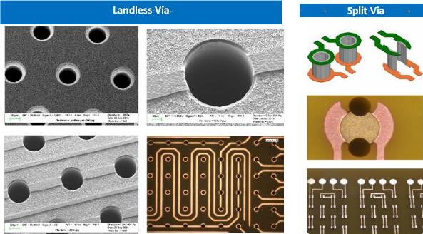
Minimum aperture: 24mil 20mil 16mil 12mil 8mil blind hole and buried hole 11.
The blind hole is the through hole that connects the surface layer and the inner layer but does not run through the whole plate, and the buried hole is the through hole between the inner layer but not visible on the surface of the finished board. the dimensions of these two types of holes can be set by reference. the article is posted by Dr.liu surong,director of Topscom pcb design layout R&D department,china Topscom provide high difficulty density & printed circuit boards PCB design & layout, mass manufacturing & fabrication,pcba boards assembly.
When applying blind hole and buried hole design, we should have a full understanding of PCB machining process, avoid unnecessary problems to PCB machining, and negotiate with PCB suppliers if necessary.
Test hole.
The test hole refers to the through hole used for ICT testing purposes, which can also be used as the through hole. In principle, the diameter of the pad should not be less than 25mi, and the center distance between the test holes should not be less than 50mil.
Component welding holes are not recommended as test holes.
two。 Setting of special wiring interval.
Special routing interval means that some special areas on the veneer need to use wiring parameters that are different from the general settings, such as thinner linewidth, smaller spacing and smaller through holes for some high-density devices, or the adjustment of routing parameters of some networks, which need to be confirmed and set before routing.
3. Define and split plane layer.
a. The plane layer is generally used for the power supply of the circuit and the stratum (reference layer). Because different power sources and strata may be used in the circuit, it is necessary to separate the power layer and the stratum, and the separation width should take into account the potential difference between different power sources. When the potential difference is greater than 12V, the separation width is 50 mil. on the contrary, 20--25mil is optional.
b. The plane separation should consider the integrity of the reflux path of the high-speed signal.
c. When the reflux path of the high-speed signal is destroyed, it should be compensated in other wiring layers. For example, the signal network can be surrounded by grounded copper foil to provide a ground loop of the signal.
b. Pre-wiring simulation (layout evaluation, to be expanded)
c. Wiring.
1. Cabling priority.
Priority of key signal lines: priority wiring of key signals such as power supply, analog small signal, high-speed signal, clock signal and synchronization signal.
The principle of density priority: start with the wiring of the most complex devices connected to the veneer. Start wiring from the densest area of the veneer.
2.Automatic routing.
If the cabling quality meets the design requirements, an automatic router can be used to improve work efficiency, and the following preparations should be completed before automatic routing:
Automatic routing control file (do file).
In order to better control the wiring quality, it is generally necessary to define the routing rules in detail before running, which can be defined in the graphical interface of the software, but the software provides a better control method, that is, according to the design situation, write the automatic routing control file (do file), software runs under the control of this file.
3. Try to provide a special wiring layer for clock signals, high-frequency signals, sensitive signals and other key signals, and ensure the minimum loop area. If necessary, manual priority wiring, shielding and increasing safety spacing should be adopted. Ensure the signal quality.
4. The EMC environment between the power layer and the stratum is poor, so it is necessary to avoid arranging signals that are sensitive to interference.
5. The network with impedance control requirements should be arranged on the impedance control layer.
6. Rules that should be followed when designing PCB.
1) ground circuit rules:
The minimum rule of the loop is that the area of the loop formed by the signal line and its loop should be as small as possible. The smaller the area of the loop is, the less the external radiation is and the smaller the external interference is. According to this rule, in the ground plane segmentation, the distribution of the ground plane and the important signal alignment should be taken into account to prevent the problems caused by the slotting of the ground plane. In the design of double-layer board, under the condition of leaving enough space for power supply, the left part should be filled with reference ground, and some necessary holes should be added to effectively connect the double-sided signals, and ground wire isolation should be adopted for some key signals as far as possible. for some designs with high frequency, special consideration should be given to the problem of ground plane signal circuit, and it is recommended to use multi-layer pcb board.
2) disturbance control.
Crosstalk (CrossTalk) refers to the interference between different networks on PCB caused by long parallel cabling.
The disturbance is mainly due to the distributed capacitance and distributed inductance between parallel lines. The main measure to overcome crosstalk is to increase the spacing of parallel wiring and follow the 3W rule.
Insert a grounded isolation wire between parallel lines. Reduce the distance between the wiring layer and the ground plane.
3) shielding protection.
In fact, the corresponding ground wire loop rules are also to minimize the loop area of the signal, which are more common in some more important signals, such as clock signals and synchronous signals; for some particularly important and high-frequency signals, we should consider the design of copper axis cable shielding structure, that is, the upper and lower of the wire is separated by the ground wire, and we should also consider how to effectively combine the shielded ground with the actual ground plane. the article is posted by Dr.liu surong,director of Topscom pcb design layout R&D department,china Topscom provide high difficulty density & printed circuit boards PCB design & layout, mass manufacturing & fabrication,pcba boards assembly.
4) the direction control rules of the alignment:
That is, the alignment direction of the adjacent layer is an orthogonal structure. Avoid moving different signal lines in the same direction in the adjacent layers, so as to reduce unnecessary interlayer interference; when it is difficult to avoid this situation due to the limitations of the board structure (such as some backboards), especially when the signal rate is high, consideration should be given to isolating the wiring layers on the land plane and isolating the signal lines on the signal lines.
5) Open-loop inspection rules for alignment:
Generally speaking, cabling (Dangling Line), floating at one end is not allowed.
The main purpose is to avoid the "antenna effect" and reduce unnecessary interference radiation and acceptance, otherwise it may bring unpredictable results.
6) Impedance matching check rules:
The wiring width of the same network should be consistent, and the change of the linewidth will cause the non-uniformity of the line characteristic impedance, and it will produce reflection when the transmission speed is high, which should be avoided as far as possible in the design. Under some conditions, such as connector lead, BGA package lead similar structure, the line width may not be avoided, the effective length of the middle inconsistent part should be reduced as much as possible.
7) routing termination network rules:
In a high-speed digital circuit, when the delay time of PCB wiring is greater than the rise time (or fall time) of the signal, the wiring can be regarded as a transmission line. in order to ensure that the input and output impedance of the signal matches correctly with the impedance of the transmission line, various matching methods can be adopted. the matching method chosen is related to the connection mode of the network and the topological structure of the wiring.
a. For point-to-point connections (one output corresponds to one input), you can choose start-to-end series matching or terminal
Parallel matching. The former has the advantages of simple structure, low cost and large delay. The latter has a good matching effect, but its structure is complex and the cost is high.
b. For point-to-multipoint connections (one output corresponds to multiple outputs), when the topology of the network is daisy chain, terminal parallel matching should be selected. When the network is a star structure, we can refer to the point-to-point structure.
Star and daisy chain are two basic topological structures, and other structures can be regarded as the deformation of the basic structure, and some flexible measures can be taken to match them. In practice, it is necessary to take into account factors such as cost, power consumption and performance, and generally do not pursue perfect matching, as long as the interference caused by mismatch is limited to an acceptable range.
8) close-loop inspection rules for wiring:
Prevent signal lines from forming self-loops between different layers. This kind of problem is easy to occur in the design of multilayer plates, and the self-ring will cause radiation interference.
9) the control rules of the branch length of the alignment:
Try to control the length of the branches, the general requirement is Tdelay < = Trise/20.
10) Resonance rules of wiring:
Mainly for high-frequency signal design, that is, the wiring length should not be an integral multiple of its wavelength, so as to avoid resonance.
11) Line length control rules:
That is, the short-line rule, in the design, the wiring length should be as short as possible, in order to reduce the interference caused by too long wiring, especially some important signal lines, such as clock lines, be sure to put the oscillator very close to the device. In the case of driving multiple devices, the network topology should be decided according to the specific situation.
12) Chamfer rules:
Acute and right angles should be avoided in PCB design to avoid unnecessary radiation and poor process performance.
13) device de-coupling rule:
a. Add the necessary decoupling capacitance to the printed board to filter out the interference signal on the power supply to make the power supply signal stable. In the multilayer board, the position of the de-coupling capacitor is generally not too high, but for the double-layer board, the layout of the de-coupling capacitor and the wiring of the power supply will directly affect the stability of the whole system, and sometimes even related to the success or failure of the design.
b. In the double-layer board design, generally speaking, the current should be filtered by the filter capacitor before being used by the device, and at the same time, the influence of the power supply noise generated by the device on the downstream devices should be fully taken into account. Generally speaking, it is better to adopt the bus structure design. In the design, we should also take into account the impact of the voltage drop caused by the long transmission distance on the device, and add some power filter loops if necessary. Avoid potential difference.
c. In the design of high-speed circuit, whether the decoupling capacitor can be used correctly or not is related to the stability of the whole board.
14) device layout partitioning / layering rules:
a. The main purpose is to prevent the interference between modules with different working frequencies and to shorten the wiring length of the high frequency part as much as possible. The high-frequency part is usually arranged in the interface part to reduce the wiring length, of course, such a layout still takes into account the possible interference of the low-frequency signal. At the same time, the segmentation of the high / low frequency part of the ground plane is also considered, which is usually used to segment the two and then connect them at a single point at the interface.
b. For hybrid circuits, analog and digital circuits are arranged on both sides of the PCB, using different layer wiring and stratum isolation in the middle.
15) isolated copper zone control rules:
The emergence of the isolated copper zone will bring some unpredictable problems, so connecting the isolated copper zone to other signals will help to improve the signal quality, usually by grounding or removing the isolated copper zone. In the actual production,
PCB manufacturers have added some copper foil to the vacant parts of some boards, which is mainly to facilitate PCB processing and to prevent PCB warpage to a certain extent. the article is posted by Dr.liu surong,director of Topscom pcb design layout R&D department,china Topscom provide high difficulty density & printed circuit boards PCB design & layout, mass manufacturing & fabrication,pcba boards assembly.
16) Integrity rules for power and ground layers:
For the areas with dense through holes, attention should be paid to avoid the holes being connected to each other in the hollowed-out area of the power supply and the stratum, resulting in the segmentation of the plane layer, thus destroying the integrity of the plane layer, and thus leading to the increase of the loop area of the signal line in the stratum.
17) overlapping power and ground layer rules:
Different power layers should avoid overlap in space. The main purpose is to reduce the interference between different power supplies, especially between some power supplies with large voltage differences, the overlap of power supply planes must be avoided, and intermediate strata can be considered when it is difficult to avoid.
18) 3W rules:
In order to reduce the crosstalk between lines, the wire spacing should be large enough to keep 70% of the electric field from interfering with each other when the line center spacing is not less than 3 times the line width, which is called the 3W rule. If 98% of the electric fields do not interfere with each other, a spacing of 10 W can be used.
19) Rule 20H:
Because the electric field between the power layer and the stratum is changing, the electromagnetic interference will be radiated outward at the edge of the plate. It's called the edge effect. The solution is to shrink the power layer so that the electric field is transmitted only within the range of the ground. Taking an H (the thickness of the medium between the power supply and the ground) as a unit, 70% of the electric field can be limited to the edge of the connecting stratum if shrinking 20H, and 98% of the electric field can be limited by shrinking 100H.
20) five-five rules:
Printed board layer selection rule, that is, clock frequency to 5MHz or pulse rise time less than 5ns, then PCB board must use multi-layer board, this is a general rule, sometimes for the consideration of cost and other factors, using double-layer board structure, in this case, it is best to take one side of the printed board as a complete ground layer.
d. Post-simulation and design optimization (to be supplemented).
e. Process design requirements.
1. General process design requirements refer to "CAD process Design Specification for printed Circuits" Q/DKBA-Y001-1999.
two。 ICT testable requirements for function boards.
a. For the veneer produced in large quantities, ICT (In Circuit Test), should be done in production in order to meet the requirements of ICT test equipment, the corresponding processing should be done in the PCB design. Generally, each network must have at least one test point for the test probe to contact, which is called the ICT test point.
B. the number of ICT test points on PCB should meet the requirements of ICT test specifications, and should be on the solder surface of PCB board, and the test point can be the solder joint of the device or through the hole. the article is posted by Dr.liu surong,director of Topscom pcb design layout R&D department,china Topscom provide high difficulty density & printed circuit boards PCB design & layout, mass manufacturing & fabrication,pcba boards assembly.
c. The minimum pad size of the test point is 24mils (0.6mm), and the minimum distance between the two separate test points is.
60mils (1.5mm).
d. For the veneer that needs to be tested by ICT, two non-metallic holes of 125MILS should be designed on the opposite corner of PCB for ICT test positioning.
3. PCB labeling specification.
The exact external dimensions of the PCB should be marked in the drilling layer, and no closed dimensions can be formed; the size and number of all holes and indicate whether the holes are metallized.
ii. Design review.
a. Review process.
After the design is completed, the PCB designer or product hardware developer can put forward the PCB design quality review according to the needs. The work flow and evaluation methods can be found in the PCB Design Review Specification.
b. Self-check item.
If you do not need to organize a review team to conduct a design review, you can check the following items yourself.
1. Check for high frequency, high speed, clock and other fragile signal lines for minimum loop area, distance from interference sources, excess holes and coils, and broken stratigraphic divisions.
two。 Check whether there is a signal wire under the crystal, transformer, optical coupling and power supply module, and avoid piercing it as far as possible, especially the grounded copper skin should be laid under the crystal as far as possible.
3. Check whether the positioning hole and positioning parts are consistent with the structure drawing, and whether the ICT positioning hole and SMT positioning cursor are added and meet the process requirements.
4. Check whether the serial number of the device is placed correctly according to the principle from left to right, and there is no screen printing to cover the pad; check that the version number of the screen print conforms to the version upgrade specification and identify it.
5. Report whether the wiring is 100% complete, whether there is a thread, and whether there is an isolated copper skin.
6. Check that the division of the power supply and the ground is correct, and the single point and common ground has been dealt with.
7. Check that the light drawing options of each layer are correct, the label and the light drawing name are correct, and the drawings that need to be pieced together only need to be marked on the drawing of the drilling layer.
8. Output the light drawing file, check and confirm the correct generation of the light drawing with CAM350.
9. Fill in the PCB design (filing) self-inspection form as required, and submit it to the process planner for process review together with the design documents.
10. Actively improve the problems found in the process review to ensure the processability, productivity and testability of the veneer.

