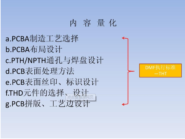
China Topscom speeched about overview of pcb assembly PCBA manufacturability design on china SMT equipment exhibition in 2021 year.
The manufacturability design of pcb assembly PCBA is not only to solve the problem of manufacturability, but also to solve the manufacturing problem of low cost and high quality. the achievement of the goal of "manufacturability" and "low cost and high quality" depends not only on design, but also on manufacturing, but also on the coordination and unity of design and manufacturing, that is,
The design of "integration". It is very important to understand this, which is the basis of pcb assembly PCBA manufacturability design. Only by recognizing this, can we master pcb assembly PCBA manufacturability design systematically and comprehensively.
In the design of manufacturability of pcb assembly PCBA, the assembly mode of pcb assembly PCBA is generally determined according to the number and package of components in (BOM), that is, the layout of components on the front and back of pcb assembly PCBA, which determines the process path during assembly, so it is also called process path design. Then, the components are laid out according to the welding process method adopted on each assembly surface. Finally, the spacing of components, the thickness of steel mesh and the graphic design of windowing are determined according to the packaging and process method.
1. Packaging is the basis and starting point of manufacturability design.
Packaging is the basis and starting point of manufacturability design. No matter the process path, component layout, or pad, component spacing, steel mesh window, are carried out around the package, it is a bridge to connect the design elements.
2. Welding method determines the layout of components.
Each welding method has its own requirements for the layout of components, for example, wave crest welding chip components, its long direction is perpendicular to the transmission direction of PCB wave soldering, and the distance is greater than the height of the components with higher adjacent components.

3. The package determines the matching between the pad and the window of the steel mesh.
The process characteristics of the package determine the amount and distribution of solder paste required. Packaging, pads and steel mesh are interrelated and influenced each other. The structure of pads and pins determines the morphology of solder joints and the ability to absorb molten solder. The design of window and thickness of steel mesh determines the printing quantity of solder paste, so the requirements of window opening and packaging of steel mesh must be taken into account in the design of solder pad.
4. Manufacturability design and SMT process determine the yield of manufacturing.
Manufacturability design provides prerequisites and inherent process capabilities for high-quality manufacturing (Cpk), which is one of the reasons why "design determines quality" is mentioned in the quality management course.
These viewpoints or logical relations are the embodiment of the internal relations of manufacturability design, and these viewpoints must be kept in mind in manufacturability design in order to carry out manufacturability design with the idea of "integration".
If u have more pcb assembly PCBA manufacturability design suggestion,pls let us know by sales@topscom.com.cn
Hello, welcome to visit our official website!
+86 13502814037 (What's up)sales@topscompcbassembly.com

Turnkey Pcba Assembly & Contract Electronic OEM Manufacturing Provider

