
China Topscom Delievered Speech About the study of pcb manufacturing (fabrication) process on 2019 China CEE Electronic Fair.
Keywords:china pcb manufacturing process,pcb board,pcba,pcb prototype manufacturing,pcb assembly
Selection of PCB substrate material.
1. Gold plated sheet (ElectrolyticNi/Au).
2.OSP board (OrganicSolderabilityPreservatives).
3. Silver plate (ImmersionAg).
4. Metal plate (ElectrolessNi/Au,ENIG).
5. Tin plate (ImmersionTin).
6. Tin spray plate.
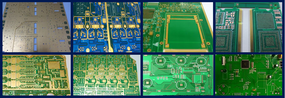
1. Gold plated plate.
The manufacturing cost of gold-plated plate is the highest of all plates, but at present, it is the most stable and most suitable for lead-free process, especially in some electronic products with high unit price or high reliability.
2.OSP board.
The OSP process has the lowest cost and is easy to operate, but the popularity of this process is still not good because the equipment and process conditions have to be modified by the assembly factory and the rework is poor. Using this kind of plate, after high temperature heating, the protective film pre-coated on PAD is bound to be damaged, resulting in a decrease in solderability, especially when the substrate is more serious after secondary resoldering, so if the process needs to go through another DIP process, At this time, the DIP side will face the challenge of welding.
3. Silver plate.
Although "silver" itself has a strong mobility, which leads to leakage, but today's "immersion silver" is not pure metallic silver, but "organic silver" co-plated with organic matter, so it has been able to meet the needs of the future lead-free process, and its solderability life is longer than that of OSP board.
4. Gold plate.
The biggest problem with this kind of substrate is the problem of "black pad" (BlackPad), so many large manufacturers do not agree to use it in the lead-free process, but most domestic manufacturers use this process.
5. Tin plate.
This kind of substrate is easy to be contaminated and scratched, coupled with the oxidation and discoloration of the process (FLUX), most of the domestic manufacturers do not use this process, and the cost is relatively high.
6. Tin spray plate.
Because the cost is low, the solderability is good, the reliability is good, and the compatibility is the strongest, but the tin spray plate with good welding characteristics can not be used in the lead-free process because it contains lead.
Printed circuit boards ((Printed Circuit Board,PCB) appear in almost every kind of electronic device. It is the carrier of all electronic devices, and there are PCB everywhere in the computer, from motherboard, graphics card, sound card to memory board, CPU board to hard disk control circuit board, optical drive control circuit board and so on. It ranges from household appliances, mobile phones, PDA and digital cameras in daily life to car electronic devices, avionics used in aircraft and highly X-capable electronic devices on satellite rockets. Living in the information age, we deal with PCB every day, and as computer enthusiasts, we talk about PCB all the time. But how is PCB made? What does the equipment that makes them look like? What is particularly important is, from what aspects to evaluate the workmanship of a board? Now, let's start our journey to PCB with these three questions.
The actual manufacturing process of PCB is completed in the PCB factory, the factory is regardless of the design, the design work is carried out by special companies, their design results are called schematics, and then the schematics are designed by professional wiring companies, and the resulting wiring diagrams are handed over to the PCB factory for production. The task of the factory is to turn the circuit diagram in the workstation into a real physical board.
What is the process from the drawing to the physical board?
Generally speaking, there are three processes: first, the preparation of production tools (Tooling); second, the specific production process; third, quality inspection (VI, electrical testing). However, both production and processing and quality control are carried out around the production process. So we focus on the production process of PCB board.
I. basic concepts to be involved in the production process.
1. Important raw materials.
Base plate.
The raw material of PCB board is copper clad substrate, referred to as substrate. The substrate is a resin board with copper on both sides. Now the most commonly used sheet metal code name is FR-4. FR-4 is mainly used in computers, communication equipment and other electronic products. The requirements for the plate: the first is the flammability, the second is the Tg point, and the third is the dielectric constant. The circuit board must be flammable and cannot be burned at a certain temperature, but can only be softened. The temperature point at this time is called the glass transition temperature (Tg point), which is related to the dimensional stability of the PCB plate. In high-level applications, customers sometimes specify the Tg point of the plate. The dielectric constant is a quantity that describes the electrical properties of the material. In the high frequency circuit, the dielectric loss (PL) of the signal is related to the substrate material, specifically, it is proportional to the square root of the dielectric constant. If the loss of the medium is large, the greater the effect of absorbing the high frequency signal and transforming it into heat is, so that the signal can not be transmitted effectively.
In addition to FR-4 resin substrates, phenolic paper substrates are also widely used in relatively simple applications such as televisions and radios.
Let's look at the composition of the substrate. The substrate is composed of substrate and copper foil, the FR-4 substrate is resin plus fiberglass cloth, and fiberglass cloth is the fabric of fiberglass. The fiberglass cloth is dipped in liquid resin and then pressed and hardened to get the substrate. In polymer chemistry, the state of the resin is divided into three states: a-stage, b-stage and c-stage. There is no close chemical bond between the molecules of the resin in a-stage, and there are few chemical bonds between molecules in b-stage, which will soften under high temperature and high pressure. C-stage is the most stable state in the chemical structure of the resin, which is solid. With the increase of chemical bonds between molecules, the physical and chemical properties of the resin are very stable. The circuit board substrate we use is made of resin in b-stage. On the other hand, the substrate is hot-pressed together with the copper foil which is located in the b-stage. At this time, the resin is in a stable c-stage.
Copper foil.
Copper foil is a conductor that forms wires on the substrate. there are two methods in the manufacturing process of copper foil: Calendering and electrolysis.
Calendering is to press high-purity copper like rolling dumpling skin into copper foil with a thickness of only 1 millet (equivalent to 0.0254mm). The manufacturing method of electrolytic copper foil is based on the principle of electrolysis, using a huge rolling metal wheel as the cathode and CuSo4 as the electrolyte to make pure copper precipitate continuously on the rolling metal wheel to form copper foil. The specification of copper foil is thickness, and the thickness of copper foil commonly used in PCB factory is between 0.3 and 3.0 mils.
PP.
PP is an indispensable raw material in the manufacture of multilayer plates, and its function is the adhesive between layers. To put it simply, the substrate sheet at b-stage is called PP. The specification of PP is thickness and resin content.
Dry film.
Photosensitive dry film is referred to as dry film, and its main component is a kind of resin which is sensitive to specific spectrum and undergoes photochemical reaction. The practical dry film has three layers, and the photosensitive layer is sandwiched between the upper and lower layers of protective plastic film. According to the chemical characteristics of photosensitive substances, there are two kinds of dry films, photopolymerization type and photolysis type. The photopolymerized dry film will harden and change from water-soluble to water-insoluble under the light irradiation of specific spectrum, while the photodecomposition is just the opposite.
Anti-welding paint.
Anti-solder paint is actually a kind of anti-solder flux, which is a kind of liquid photosensitive material which has no affinity to liquid solder. like photosensitive dry film, it will change and harden under the light of specific spectrum. When in use, the anti-solder paint should also be mixed with the hardener. Anti-solder paint is also called ink. The color of the PCB board that we usually see is actually the color of the anti-solder paint.
Negative film.
.
The negatives we are talking about are similar to photographic negatives, which are all materials that use photosensitive materials to record images. The customer sends the designed circuit diagram to the PCB factory, and the workstation in the CAM center outputs the line diagram, but not through a common printer, but by a light plotter (Plotter, figure 1), whose output medium is the film, also known as film (film). The place where the film is exposed is black and opaque, otherwise it is transparent. The negative plays an important role in the PCB factory. All the things on the substrate must be turned into negatives in order to achieve the principle of image transfer.
2. Composition of PCB board.
Let's get to know the circuit board we have. From the manufacturer's point of view, the circuit board is layered, sandwiched inside is the inner layer, exposed to the outside can weld a variety of accessories called the outer layer. The outer layer of the inner layer is composed of wires, holes and PAD. The wire is the copper wire that plays a leading role, and the hole is divided into the through hole (Plating hole) and the non-through hole (None Plating hole), which is referred to as PT and NP respectively. The PT hole includes a part hole (Component hole) inserted into the IC pin and a copper as a conduction medium on the hole wall connecting the through hole (Via hole), PT hole between different layers; the NP hole includes a mechanical hole for fixing the plate card, and the hole wall is copper-free. PAD is a general term for the copper ring around the PT hole and the welding pad of the IC pin on the board surface. In addition, the two sides of the circuit board are used to be called Compplane and Sold surface. This is because one side of the circuit board always acts as the mounting surface for all kinds of electronic components.the article is posted by Mr.Xiao Wei, Director of Topscom Pcb Layout Design Department,China Topscom provide professional Pcb boards layout design,pcb assembly and manufacturing,full turnkey systems integration box build assembly,contract electronic manufacturing service.
3. Image transfer.
.
How is the circuit on the circuit board made? Why can the circuit on the negative become real copper on the circuit board? This process is through image transfer, that is, the use of photosensitive materials to transfer patterns from one medium to another. Take the production of the inner circuit as an example: the substrate should first be pressed with a layer of photosensitive dry film, and then covered with the film, and then exposed to see the dry film. The place where the light is illuminated is very different from that where it is not illuminated. For photopolymerized dry film, the color of the place exposed to light becomes darker, which means that it has hardened (as a result of photopolymerization), and then after development (washing the unhardened dry film with sodium carbonate solution), the transparent place on the original film can be retained, while the original film is black, and the dry film has been developed because it has not been hardened. When the substrate is etched with copper etching solution (a chemical that corrodes copper), the copper without dry film protection is completely destroyed, while the copper surface under the dry film is retained. If we use colorless transparency on our film to represent lines and copper areas, and black to represent copper-free areas, after exposure, development, and etching, the image on the film will be transferred to the substrate (figure 2). The overall result is that the circuit diagram in the CAM workstation is transferred to the negative through the Plotter output, and then transferred to the substrate through the above process. The method of image transfer is widely used in PCB factory. It has the opportunity to show its ability not only in the production of lines, but also in the production of anti-welding, screen plates and other occasions where precise control of graphics is needed.
4. Multilayer plates are manufactured by adding layers.
How are multilayer plates made? We know that the circuit board is layered, and the board in the computer has both double panels and multi-layer boards. For example, most motherboards are four-or six-layer boards (now most of them are four-layer boards, mainly to reduce costs). The practice of double-panel is better to imagine, the substrate naturally has two sides, while the multi-layer plate is to "stick" multiple double-panel together. Take a four-layer plate as an example, first use a substrate to make one or two layers, then use a substrate to make three or four layers, and then combine the two into a four-layer board. How to bond it? Binder is the raw material mentioned above-PP, with the help of the high temperature and high pressure environment of the pressing machine, PP softens at first and then hardens, changing from b-stage to c-stage to merge the two double panels into one. You can also make the second and third layers located on the inside. Before pressing, the second and third layers are covered with PP, and then covered with copper foil, and then pressed to get the same four-layer plates. This difference is called the choice of laminated structure. The manufacturing method of this kind of multilayer plate is called adding layer method. What I want to tell you is that you can tell whether a board is double-faced or multilayer from the outside, but it is impossible to tell how many layers there are in a multilayer. For the multilayer, you will see that the inside of the board is black through some areas of the substrate that are not coated with anti-welding paint, and that is the color of the inner layer. I'll explain why it's black later.

