
Mythbusting: PCB Layout
Printed Circuit Boards (or PCBs for short) have been an integral part of circuit design for many years. In fact, it’s because of these PCBs that we’ve been able to satisfy our need to make devices slimmer and smaller.Owing to their meteoric rise in popularity, the public knows close to nothing about what PCBs are and how they operate. This has led to the circulation of misinformation on the subject matter which does nothing but confound the reader.
We’ve decided to address this serious issue head-on which is why today we’ll be discussing and debunking a few common myths associated with PCB layout and design.
Myth #1 – Every PCB Layout Is The Same:
People who offer crash courses on PCB design and implementation will have you believe that every PCB ever created has the same layout. This is nothing but an unethical advertising tactic to get you to sign up for their inferior courses.The Truth: All PCBs are unique in some way, shape, or form. Granted the technique used to create a PCB might be similar but even that varies from one type of PCB to another. Make no mistake about it; PCB design is a complicated business that should never be taken lightly.
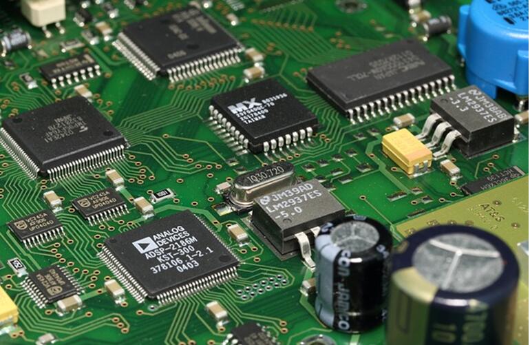
Myth #2 – All PCBs Are Green:
For some reason people have been led on to believe that all PCBs are primarily green in color. This rumor originates from the fact that most PCBs you see on display at electrical stores are green-colored.The Truth: The color of the PCB has no impact whatsoever on the performance of the PCB. In other words, you can easily find a blue PCB that outperforms its green counterpart and vice versa. When it comes to performance, the placement of components and wire mapping is all you need to concern yourself with.

Myth #3 – The Wire Mapping Doesn’t Matter:
It baffles us to see people confidently state that the mapping of the wire and the placement of electrical components has little consequence on the performance of the PCB. What’s even more incredible is the vast majority of people who blindly trust this piece of information and think of it as a fact.The Truth: The mapping and placement of the wires and is a crucial part of PCB design. How you route and map your wires will have a direct impact on how long it takes for a signal to reach an electrical component, so, be very careful when mapping your PCB.
Myth #4 – The Work Is Done Once The Schematic Is Finalized:
By far the most common rumor that we hear as far as PCB layout and design is concerned is that the work is done as soon as a schematic is finalized. Turns out, this is far from the truth.The Truth: Contrary to popular belief, your work is far from over once the electrical schematic has been finalized. In fact, the hard work is just getting started as you have to troubleshoot and double-check the position of every component on your circuit board.
After that begins a complicated process of going through many checks and balances before your design can be deemed suitable for mass production.

Owing to the complications associated with the process, countless organizations and individuals have turned to PCB manufacturing companies to create their electrical and electronic solutions. In recent years, Topscom PCB Assembly has emerged as the go to choice of people looking for robust and reliable SMT PCBs.
So, if you want to use premium quality PCBs in your circuits, pick up the phone and get in touch with Topscom PCB Assembly.

