
Abstract: because of the stringent requirements of the automobile environment, automotive electronic products must have the following characteristics: (1) strong environmental adaptability. The climatic environment of automobile use is very different, which objectively requires electronic products to adapt to the harsh climatic environment such as high temperature, high humidity, severe cold and hot heat, and at high temperature of 70 "C, low temperature of-20 c or temperature of 40" C and humidity.
It works normally at 95%. (2) strong anti-vibration and anti-impact ability. Car driving must adapt to various road conditions, including a flat road and a mountain road, so it objectively requires that the electronic products installed on the car have strong anti-vibration and anti-impact ability, and must work normally under the conditions of triaxial acceleration 1.5g, upper and lower amplitude up to 5mm or impact acceleration 50g, impact time 6 ms. (3) the reliability of the product is high. Automotive electronic products must meet the three-package period of 100,000 kilometers or two years, so they have higher requirements for the quality of automotive electronic products. the article is posted by Dr. Lee Duang, Senior Vice President of Topscom Technology Automotive EMS Department,china Topscom provide one stop shop turnkey automotive electronic device pcba assembly contract electronic manufacturing services.
In view of the characteristics of more than 1000, the quality control of the manufacturing process of automotive electronic products is very strict, in which manufacturability design is the premise of ensuring a high quality level of automotive electronic products. here are some of our experiences in applying manufacturability design to automotive electronic products for reference.
Keywords: Tg (glass transition temperature); process edge; heat insulation; self-calibration force; test point; automotive electronics wiring;automotive pcba boards assembly.
1 the definition of manufacturability design and the significance of its development.
Design for manufacturability ((Des i gn For Manufacture,) is referred to as DFM), which refers to the design with easier manufacturing and lower manufacturing cost. it mainly studies the relationship between the physics of the finished product and the various parts of the manufacturing system, and applies it to the product design in order to integrate the whole manufacturing system for overall optimization, which is the most effective way to ensure the quality of PCB design.
DFM questions involve many links in the PCB industry chain-designers, PCB boards manufacturers, pcb assemblers, test manufacturers and system manufacturers. In the process of looking for a solution, people in the industry realize that it is the lack of 1000 standards that leads to poor communication between various links, so that the design level of the whole PCB industry in China is low and the production capacity is not high.
The harm of bad design in the production and manufacture of pcb smt assembly includes:
(1) causing a large number of welding defects;
(2) increasing the workload of board repair and re-repair, wasting man-hours and delaying the construction period;
(3) increasing the process of processing, wasting materials and resources;
(4) repair may damage components and printed boards;
(5) the reliability of the product is affected after repair;
(6) cause poor manufacturability, increase the difficulty of the process, affect the utilization rate of equipment, and reduce the efficiency of production;
(7) when the production is serious, it needs to be redesigned, which prolongs the actual development time of the whole product and loses the opportunity of market competition.
According to the D-4 survey of HP Company, the total product cost depends on the original design of thousands of products, and 75% of the total product cost depends on the original design of thousands of products.
It depends on thousands of design instructions and design specifications. 70 "'80% of production defects are caused by thousands of design reasons. With our company's.
. for example, before the manufacturability process audit of the product is carried out, the product is generally modified more than 5 times.
And it is unable to improve the quality of the product, and the problems of false welding and tablet erection of the components have never been well improved, and even the embarrassment of having to change the board because the product cannot be manufactured, whether it is the product development cycle, manufacturing cost, or product. the article is posted by Dr. Lee Duang, Senior Vice President of Topscom Technology Automotive EMS Department,china Topscom provide one stop shop turnkey automotive electronic device pcba assembly contract electronic manufacturing services.
Quality, can not form an advantage in the industry, resulting in low competitiveness of products.
2 how to carry out manufacturability design in automotive electronics enterprises an enterprise to implement DFM, should include three parts:
First, the renewal of ideas. With regard to the quality problems caused by thousands of design defects, some senior engineers tend to have their own ideas and are unwilling to accept others to point out their design defects to correct them, or even say that they are manufacturing capacity problems. this not only requires design engineers to change their original ideas, but also business leaders need to realize the importance and necessity of manufacturability design. Because the implementation of DFM is an inter-departmental system engineering, it requires the design and manufacturing departments to break the door view and establish a team with the participation of relevant departments.
Second, the establishment and maintenance of system resources. Due to the lack of standards, designers generally design according to their own preferences and habits. once designers change, the design of a circuit board needs to be completely redone, including material selection, layout and wiring and so on. invisible in the waste of a lot of manpower and material resources. According to the equipment conditions of our company and the characteristics of our products, it is very important to establish a set of design specifications and databases suitable for our use. Automotive electronic products have great commonness in structure and composition. Therefore, it is also important to consider how to achieve collinear or mixed-line production in design standards in order to improve production efficiency. How to do a good job of the standard, that is, a standard that designers and manufacturers should abide by together, and implement it according to this standard, is a very important part of DFM.
Third, it is the application and implementation in the process of new products. Established design specifications should form documents and databases, which should be followed by many developers, designers and manufacturing engineers in the process of new product development. Effectively ensuring that the specification can be well followed and implemented is an issue worthy of attention, and it is necessary to train engineers on a regular basis to require them to have a good grasp and a deep understanding of the specified requirements. In addition, establish a comprehensive review list and review it according to the items in the list by a specialized engineer to help the development engineer find
(l) Selection of PCB board material. The substrate with higher Tg (glass transition temperature) should be selected, generally speaking, 130T,
140t, 150t and 170t are optional, Tg should be high thousand circuit operating temperature is necessary, at the same time, the demand of production process should also be taken into account. The heat resistance of PCB requires that PCB boards have a heat resistance of 250 t for 50 s.
(2) the design of the jigsaw puzzle. According to the characteristics of the product and the consideration of production efficiency, the appropriate splicing method should be selected, and the unreasonable use of V-CUT, in X direction should be avoided in order to avoid large bending deformation of PCB after passing through the reflux furnace, resulting in PCB card and AOI can not be detected. Generally speaking, when the length in X direction is lower than 1000 120mm, it is easy to produce the phenomenon that PCB transmission is not smooth.
(3) the design of the process edge. The width of the process edge is recommended to be 7 -10 mm. For the thousand-side mounting board, the components cannot be arranged within 3 mm from the edge of the board, which is determined by most of the tracks of the printing press and the placement machine. For the PCB with thousands of double-sided patches, the length of the PCB furnace part supported by the chain of the thousand reflux furnace is generally 6 mm "'7 mm, so the distribution of components within this range is not allowed. At the same time, in order to provide enough convenience for the production operation, it is necessary to print arrows on the edge of the process.
Head instructions to guide the operator's work.
(4) the design of MARK point. It is preferred to have a circular mark with a diameter of 1.5 mm, and the equipment also requires a distance of PCB from the MARK point.
The distance between the edges should be greater than or equal to one thousand four mm.
* put three PCB benchmark marks MARK on the PCB, all on the corner of the PCB, considering that once the PCB enters the board in the opposite direction, the equipment can automatically identify, the distance from the RK point to the top of the corresponding corner should be inconsistent, and it is better to ensure that there is a gap between the left and the right of 2mm.
Around the MARK point, considering the contrast between the welding resistance material and the environment, there should be 1-2mm dishes unhindered welding around the MARK; do not be careful not to set the MARK on a large area of the network, so as not to cause interference, resulting in poor recognition of the equipment residence.
(5) the design of positioning hole. General screen printing machine, placement machine for PCB positioning in addition to the above-mentioned edge positioning port two edge), there are hole positioning, especially if there are AI components, the positioning hole requirements are very strict, once failed to comply with the requirements, there will be PCB can not be transmitted or transmission is not in place, PCB floating and other dangerous situations. Generally speaking, the hole diameter is 4mm, the location of the positioning hole is at the 5mm of each side of the PCB.
(6) the design of the pad.
* the following key elements should be mastered in the design of rectangular chip pads:
A the symmetry of the pad-both ends must be symmetrical in order to ensure the balance of the surface tension of the molten solder. You should know,
A large number of defects in the SMT process are caused by the imbalance of surface tension between a thousand sides.
B the spacing of the pads ensures that the ends or pins of the components are properly lapped with the pads. In order to obtain high-precision self-calibration force, it is best to protrude 0. 5% to the inside corresponding to the size of the pad at the lower end of the electrode of the mounting part. 1 "'0. at the 2mm level, a good self-calibration force can be obtained.
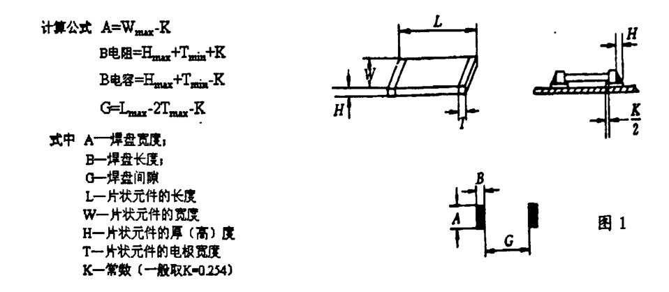
(2) the design requirements of the pads for rectangular sheet components, as shown in figure 1:
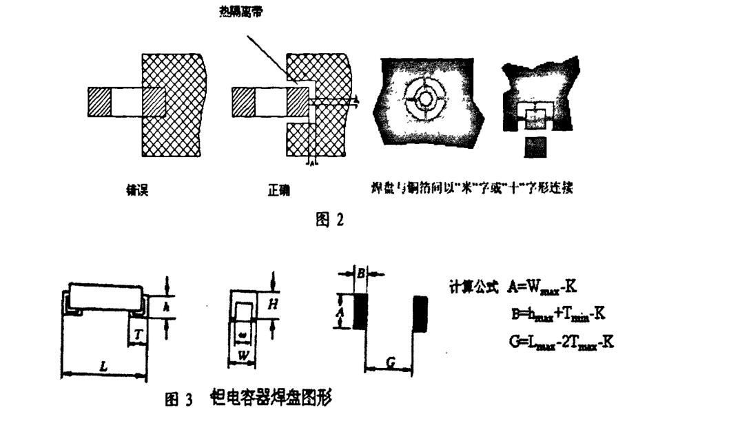
(3) the large area copper pin is required to be connected to the pad with a hot belt.
In order to ensure good tin penetration, the pads of the components on the large area copper pins are required to be connected to the pads with heat insulation.
Thermal insulation pads cannot be used for pads with high current over 5A, as shown in figure 2:
(4) huge capacitance.
The end electrode of the giant capacitor is not directly wrapped in the end of the body, but the body drawn by the metal sheet, and then bent, the width of the metal is small, the width of the body, and the width and height of the weldable end of this kind of element, depending on the packaging form and the supplier, it is likely that the width and height of the body of the small element, as shown in figure 3. Therefore, when calculating the capacitance with the formula shown in figure 3, use h instead of H to show the difference.
In SMT pcb boards assembly, the graphic design of the pad of the small form factor package transistor (SOT) is relatively simple. Generally speaking, it is only necessary to follow the following rules: the center distance between the pads is equal, and the welding between the pads and the device leads is equal. the article is posted by Dr. Lee Duang, Senior Vice President of Topscom Technology Automotive EMS Department,china Topscom provide one stop shop turnkey automotive electronic device pcba assembly contract electronic manufacturing services.
The joint is similar, but it should be expanded by 0. 5% in the direction of length. 381, it should be reduced by 0. 5% in the width direction. three hundred and eighty one. Attention should be paid to the varieties of SOT, such as SOT- 23, SOT- 89 and so on. Figure 4 shows the reference drawing of the pad.
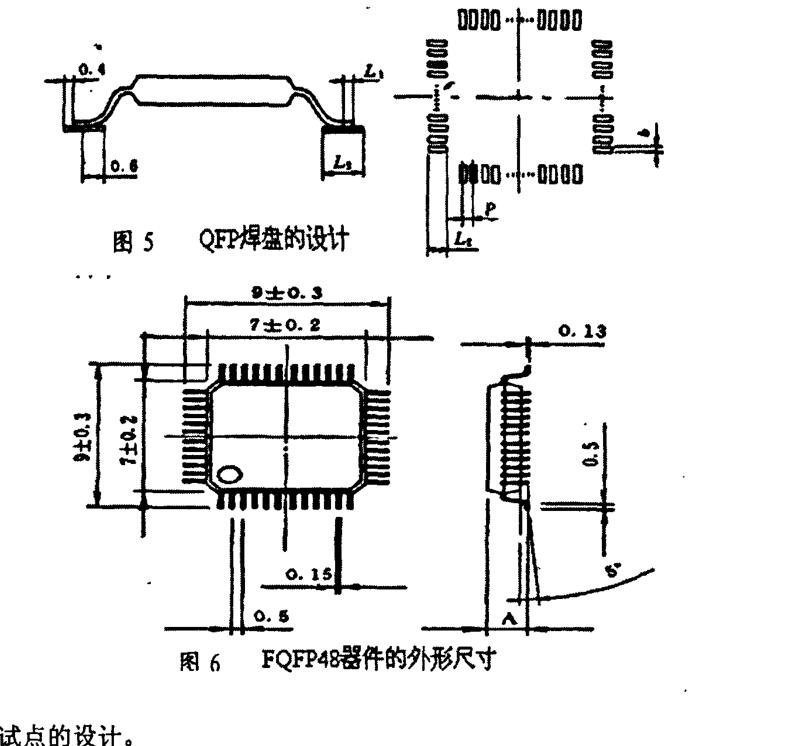
(6) QFP pad design.
A) calculation of pad length.
The best ratio of pad length to pin length is: L2 / L _ 1 / 2. 5 / L _ 1 ~ 3:1 or L2=F+Ll+A (F is the front 0. 4; A.
For the backend 0. 6; L1 is the pin length of the device; L2 is the pad length), 0. 5 in figure 5. 4 and 0. (6) the two dimensions are adjusted according to the actual situation of the device.
B) calculation of pad width.
The width of the pad is usually 0. 49 Less than or equal to b Less than or equal to 0.54p (P is the nominal size of the pin, b is the width of the pad), and the center distance of the thousand pins is 0. 5 mm QFO pad design, if you take the FQFP48 device as an example, its size is shown in figure 6.
(7) the design of the test point.
(!) PCB boards can set up several test points, these test points can be holes or pads, and evenly distributed;
@ the setting of the test hole is the same as that of the reflow soldering guide hole.
@ the surface of the test pad is the same as that of the surface mount pad.
Try to use one side test to avoid needle bed test on both sides.
@ probe test support through hole and test point requirements:
When using on-line testing, several probe test support through holes and test points should be set on the PCB. When these holes or points are connected to the pad, they can be drawn from anywhere about the wiring, but pay attention to the following points:
* pay attention to the minimum distance between probes of different diameters for automatic on-line testing;
* the through hole cannot be selected in the extended part of the pad, which is the same as the requirement of the through hole in reflow soldering.
* the test point cannot be selected on the solder joint of the component or on the body of the component, the correct way is to contact the probe with the lead-out pad;
* the diameter of the pad tested by the probe is not less than 1000. 9 mm .
* the gap around the test needle is determined by the assembly process. The minimum gap is equal to 80% of the height of adjacent components, and the minimum is.
0. 6 dishes.
* on the probe side of the PCB, if the part height does not exceed 5.7 mm, the test tooling must give way and avoid the high components, so the pad must be kept away from the high component 5 mm.
* Golden hand is not used as a test point to avoid damage.
(8) basic alignment size requirements:
Minimum linewidth of copper pin: single panel 0. 3 mm, double panel 0. The minimum copper pin on the edge of 2 mm; is 1. 0 mm.
Minimum line gap of copper box: single panel: 0.3 mm, double panel: 0.2 mm.
The alignment of the pad should be able to make the pad form a regular pattern, not on the inside of the two pads and at any corner of the pad, as shown in figure 7.
The above are some of the design requirements, in order to achieve a good PCB manufacturability design, design audit is very important, first of all, the designer self-audit, and then by the process personnel to review item by item, after the completion of the audit, there must be an audit report, put forward modification suggestions, modify after consultation with the designer, and finally must be approved by the competent technician. A review meeting should be organized at each stage. It is necessary to follow the process audit procedure to operate, if it does not follow the process, it will often cause unnecessary board changes, and the steel mesh and tooling used in trial production will often cause waste, which not only increases the manufacturing cost, but also prolongs the product development cycle.
The format of the audit report can be designed according to the specific conditions and requirements of our company, but DFM is used uniformly throughout the company.
Report template, the report template is clear and hierarchical, clear at a glance, so that people know the existing problems and importance. The report mainly includes: customer name, product name, PCB description, problem severity level (very serious 4, more serious 3, general 2, reminder l, qualified 0), responsible person, tracking status, etc.
Examples of the format of the audit report are as follows:
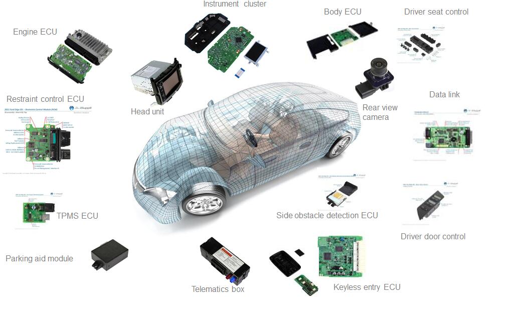
Automotive System Devices Equipments, Vehicular Electronics, pcb assembly & electronics contract manufacturing services supplier: china Shenzhen Topscom, with ISO certified 16949 Certification.experienced automotive PCBA Assembly elements products include: engine ECU,Restraint control ecu,instrument cluster,body ECU,Driver seat control,TPMS ECU,Packing and Module,head unit,rear view camera,data link,side obstacle detection ECU,driver dorr control,telematics box,keyless entry ECU etc.
China Topscom has the capability to provide in-house manufacturing for key automobile and vehicle electronics elements such as RF, optical memory components, cable assemblies, PCB board, PCBA assembly, PCBA assembly, sub-assemblies and finished product full systems integration box build assembly.
Volume Production Experienced Products As Below By Topscom:
• Wiper controllers
• Vehicle access and immobilizing systems
• Transmission controls
• Telematics
• Server based global navigation systems
• Sensor and switch assemblies
• Seat heater controls
• Power steering controls
• Multimedia in-dash receivers
• Instrument panel cluster assemblies
• In-car entertainment systems
• Ignition modules
• High density light modules
• Hands-free cellular communicators
• Engine control modules
• Driver information systems
• Cooling system modules
• Climate control modules
• Body controllers
• Audio systems
• Alternators
• Alternate fuel modules
• Vehicular Electronics
• Body Controllers
• Meter Clusters & Steering Column Electronics
• Climate Controls & Blower Assemblies
• Advanced Driver Assistance Systems
• Park Assist & Intelligent Sensors
• LED Lighting Systems
• Head Units, GPS & Infotainment Systems
• Electric Vehicle Control Units & Inverters
• Remote Controls & Toll Tags
• Communication Controls, Amplifiers & Tuners

