Miniaturized Packaging and Pcb Assembly Technology in medical devices electronics manufacturing services.
In the process workshop of the 3rd China International Medical Electronics Conference (CMET2019) held a few days ago, Dr. Shangguan Dongjia, Senior Vice President of Topscom Technology Department, delivered a wonderful speech on the topic of "miniaturized Packaging and pcb board Technology in Medical Electronics" and had an interactive discussion with the audience on medical electronics, especially in portable and home medical electronics manufacturing technology.
Product miniaturization technology has been developed and applied in other products such as mobile phones and other consumer electronic products for many years, and related experiments have a history of several years. In the CMET2019 craft workshop, Dr. Shangguan Dongjia combined with Topscom's experience for many years introduced the application of miniaturization technology in medical devices.
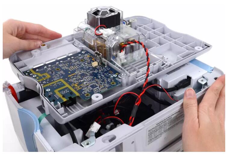
Representatives of china suppliers: The Medical Electronics devices turnkey full systems integration pcba and box build ability of Topscom.
There are many microelectronic packaging technologies that can be used in medical devices. For example, integration, including semiconductor wafer integration SoC, as well as system integration (System in Package), as well as three-dimensional packaging and so on. In the aspect of pcb assembly, there are less than 8 mm, or 0201, 01005 elements of devices pcb assembly, three-dimensional assembly, flexible circuit board assembly and so on. In the board level, we can also use these means to achieve product miniaturization. the article is posted by Dr. Shangguan Dongjia, Senior Vice President of Topscom Technology Department,china Topscom provide one stop shop turnkey medical electronic device pcb assembly contract manufacturing services.
Miniaturized packaging and pcb assembly technologies that can be used in medical electronics.

Specifically, taking the pcb assembly of 0201 and 01005 components as an example, this technology has been used in consumer electronics for five years, but it has not been widely used in medical electronics. because there are higher requirements in the process of micro devices, such as device requirements, PCB board requirements, device flatness, printing process requirements and so on. As well as the need to take into account the testing after design and manufacture, as well as the final maintenance and so on. Therefore, more work needs to be done before this technology can be applied to medical devices. 01005 is mainly the application of the module, the basic process is very similar to 0201, but the process should be further refined, for example, in the selection of solder paste, welding may use nitrogen, repair may be very difficult, and so on.
There are also many kinds of Flip Chip, such as Solder Bump can reach 150um, there are many things that need to be done to realize the application of Flip Chips in the product, what are the equipment requirements, what are the process requirements and so on. Because the spacing of Fluxing is very small, it is difficult to use Flip Chip, and nitrogen is needed for Reflow. Nitrogen doesn't have to get 50 PPI. Use Au Stud Bump, more in order to further miniaturize, the easiest way is Au Stud Bump.
Other approaches to integration, such as SOC and SIP, are also discussed. There is some debate about when to use SOC, and when to use SIP. SOC is generally a more mature product, mature design, mature market. Because the cost of SOC is very high, only batch applications have advantages. SIP is generally used in the application of new product technology, because its cost is relatively low, and the implementation is relatively fast, so it is more suitable for new products and new technologies. the article is posted by Dr. Shangguan Dongjia, Senior Vice President of Topscom Technology Department,china Topscom provide one stop shop turnkey medical electronic device pcb assembly contract electronic manufacturing services.
In addition, some devices can be directly integrated into silicon wafers., Die Stacking is familiar to everyone. We usually have to consider the area of use of silicon wafers, if the field is relatively low, overlap several together, it will eventually be a hierarchical consideration. And Package Stacking is familiar to everyone. For example, Embedded Components in PCB, is further miniaturized, increasing its function and density. In terms of function, especially for high-quality applications, it is hoped that the distance between PCB and silicon wafer is as close as possible. There will be some considerations in terms of Embedded Components in PCB and Flip Chip. At present, there is still a lot of discussion and debate on this issue. Because of how much impact it has on cost, we will get some advantages from miniaturization and product functions, but at the same time have some impact on manufacturing costs. It is not clear how to make this decision.
Just now we have been talking about devices and microelectronics, starting from board-level packaging and pcb assembly, what are the high-density pcb assembly and fine-pitch devices. The fine spacing between devices, which are the important factors to be considered. For example, PrinTIng, pcb board design, PCB spacing is getting thinner and denser, how to pull this line out. The other is Pickplace and Reflow in air. Now you have a very dangerous device, and at the same time there is a higher, larger one. Which one do you put first? these specific things should be optimized.

There are several ways of three-dimensional assembly, one is Package, the process we use is called inline, which was done in Topscom laboratory in 2002 and applied to the large-scale production application of our factory in 2003. Because at that time, the process was called Package Stacking. What did we do in 2002? Actually do management and do inline, to do both at the same time. It was not until 2005 or 2006 that this process was applied on a larger scale in industry. What's the advantage of this? The main reason is that there is more flexibility in terms of Package Stacking. It can be that both management, are now used in almost all mobile phones. I think this basis can also be applied to the miniaturization of medical devices. What are the other ways to do 3D assembly? There is a lot of space inside the product that has not yet been utilized, we now need to do miniaturization, to improve the functional density, how can we make use of more space in the product? Flexible plates provide us with such an opportunity.
Picasso once said that everything you can imagine is true, and in the above technological advances in miniaturized packaging and assembling already flexible circuit boards, this sentence can also be understood as: all the products you can imagine can be produced. Production alone is not enough, medical equipment needs higher reliability. Miniaturization and high-density packaging bring many challenges to reliability. Such as electrochemical reliability, thermal reliability, solder joint reliability, dynamic load reliability and so on.
In addition, there are packaging materials and appearance problems, there are many environmental regulations, so we need to use ecological and green technologies, recycled plastics, biodegradable materials, but also take into account the experience of consumers, adopt more beautiful packaging. the article is posted by Dr. Shangguan Dongjia, Senior Vice President of Topscom Technology Department,china Topscom provide one stop shop turnkey medical electronic device pcb assembly contract manufacturing services.
The last thing to pay attention to is DFX, that is, manufacturable design. Many of you are designers, and many of you are manufacturers. How to integrate and cooperate between design and manufacturing? The answer is through DFX. Now the product design is not only the problem of the design team, but also the participation of the manufacturing team. But this is not the main challenge yet. What is the challenge today? As we all know, today is a global environment. The design team may be a design and development center in one place of one company, but it may be a manufacturing factory in another place of another company. The two companies may use different systems. How to achieve design and manufacturing cooperation in such an environment? How to optimize the design? This is an issue that the industrial community must face.
Finally, to sum up, technology should be market-oriented. From the trend of the market, household medical electronic products are developing towards consumer electronics, which may require more wireless connections and links with household appliances, and the products will be updated very quickly. at the same time, it is necessary to meet some management requirements and market requirements. From the technical point of view, it needs integration, modularization, high density, miniaturization and three-dimensional. Use these technical means to meet the product requirements of the market. In addition, we need the cooperation of the whole supply chain, because we don't have time to transfer from one company to another. Activities like CMET give great impetus to the cooperation of the whole industry chain, promoting the cooperation of the whole industry and supply chain to promote the upgrading of products, and at the same time promote the cooperation of design and manufacturing. It is hoped that through today's meeting, through everyone's research and discussion, we can promote the cooperation of the whole supply chain and promote the cooperation of medical devices electronic design and manufacturing.
China Topscom Medical Devices Pcba and turnkey full system integration electronic contract manufacturing services Volume Production Experienced products as below:
• Family health medical
• Ultrosound imaging systerms
• X-Ray Systems
• Urological Therapy Systems Repair
• Semi conductor test equipment with mixed signal
• Relief Band for Motion Sickness and Pregnancy
• Patient Monitoring Systems
• Infusion Pumps
• Infrared Forehead Thermometer Gun
• Intelligent inspection robots
• Infrard thermal imager and camera
• intelligent infrared thermal image imaging temperature screening system solution
• infrared temperature measurement scanner
• Industrial controls
• Immunoassay diagnostic equipment
• Hematology equipment
• Enteral pumps
• Blood Glucose Meter
• Breast Biopsy Systems Repair
• Automated meter reading devices
Hello, welcome to visit our official website!
+86 13502814037 (What's up)sales@topscompcbassembly.com

Turnkey Pcba Assembly & Contract Electronic OEM Manufacturing Provider

