China Topscom Delivered Article About production process control of high difficulty multilayer pcb circuit boards manufacturing on 2020 china PCB world Magazine.
Keywords:China printed circuit board assembly Industry,pcb board,pcb assembly.
High-level pcb circuit boards are generally defined as high multi-layer pcb circuit boards with 10 ~ 20 layers or more, which are more difficult to process than traditional multi-layer circuit boards and require high quality and reliability. it is mainly used in communication equipment, high-end servers, medical electronics, aviation, industrial control, military and other fields. In recent years, the demand of high-level board market in application communications, base station, aviation, military and other fields is still strong, but with the rapid development of China's telecom equipment market, the prospect of high-level board market is promising.
At present, the domestic PCB manufacturers that can mass produce high-level pcb circuit boards mainly come from foreign-funded enterprises or a small number of domestic-funded enterprises. The production of high-level circuit board needs not only higher input of technology and equipment, but also the experience accumulation of technicians and production personnel. at the same time, the formalities of customer authentication of high-level circuit board are strict and tedious, so the threshold for high-level circuit board to enter the enterprise is high. it takes a long production cycle to realize industrialization. The average number of PCB layers has become an important technical index to measure the technical level and product structure of PCB enterprises. This paper briefly describes the main processing difficulties encountered in the production of Multilayer circuit boards, and introduces the control points of the key production processes of Multilayer circuit boards, which can be used as a reference for colleagues.
1, the main difficulties in production.
Compared with the characteristics of conventional circuit boards, high-level circuit boards have the characteristics of thicker parts, more layers, denser lines and through holes, larger unit size, thinner dielectric layer and so on. Inner layer space, interlayer alignment, impedance control and reliability requirements are more stringent.
1.1 difficulties in alignment between layers.
Due to the large number of high-level plates, the customer design side has more and more strict requirements for the alignment of each layer of PCB. Usually, the interlayer alignment tolerance is controlled by ±75 μ m. Considering the factors such as the large size design of Multilayer plate units, the environmental temperature and humidity of the graphics transfer workshop, as well as the dislocation superposition and interlayer positioning caused by the inconsistency of different core layers, it is more difficult to control the interlayer alignment of Multilayer panels.
1.2 difficulties in making inner circuit.
The Multilayer board adopts special materials such as high TG, high speed, high frequency, thick copper and thin dielectric layer, which puts forward high requirements for inner circuit fabrication and graphic size control, such as the integrity of impedance signal transmission, which increases the difficulty of inner circuit fabrication. The width of the line is small, the open short circuit increases, the micro short increases, and the qualified rate is low; the signal layer of the fine line is more, the probability of missed detection of the inner AOI is increased; the thickness of the inner core plate is thin, which is easy to wrinkle and lead to poor exposure, and it is easy to roll up when etching through the machine; most of the high-level boards are system boards with large unit size, and the cost of scrapping the finished product is relatively high.
1.3 difficulties in pressing production.
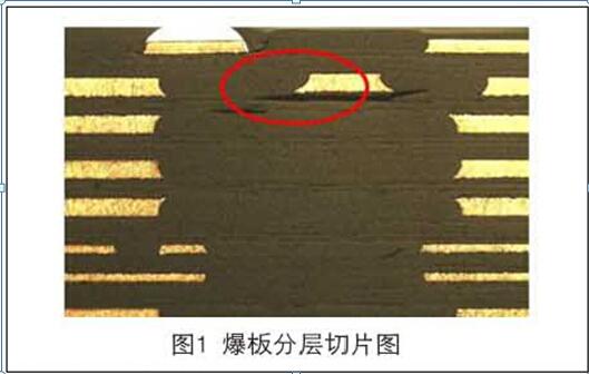
When multiple inner core plates and semi-solidified sheets are superimposed, it is easy to produce defects such as skateboard, delamination, resin cavity and bubble residue during pressing production. When designing the laminated structure, it is necessary to fully consider the heat resistance, voltage resistance, glue filling capacity and medium thickness of the material, and set a reasonable pressing program for the Multilayer plate. Due to the large number of layers, the control of rise and shrinkage and the compensation of size coefficient can not be consistent, and the thin layer of interlayer insulation can easily lead to the failure of interlayer reliability testing.
1.4 difficulties in drilling.
Special copper plates with high TG, high speed, high frequency and thick copper are adopted, which increases the difficulty of drilling roughness, drilling burr and decontamination. Many layers, cumulative total copper thickness and plate thickness, drilling tool is easy to break; dense BGA, narrow hole wall spacing caused by CAF failure; plate thickness is easy to lead to oblique drilling problem.
Control of key production processes.
2.1 material selection.
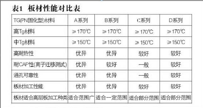
With the development of high-performance and multi-functional electronic components, it also brings high-frequency and high-speed signal transmission, so electronic circuit materials are required to have relatively low dielectric constant and dielectric loss, as well as low CTE, low water absorption and better high-performance copper clad laminate materials to meet the processing and reliability requirements of Multilayer laminates. The commonly used plate suppliers are mainly A series, B series, C series and D series. The comparison of the main characteristics of these four kinds of inner substrate is shown in Table 1. The semi-solidified sheet with high resin content is selected for the Multilayer thick copper circuit board, the flow amount of the interlayer semi-solidified sheet is enough to fill the inner layer pattern, and the insulating dielectric layer is too thick, on the contrary, the insulating dielectric layer is too thin. it is easy to cause quality problems such as dielectric delamination and high voltage test failure, so it is very important for the selection of insulating dielectric materials.
2.2 Design of laminated structure.
The main factors considered in the design of laminated structure are the heat resistance, voltage resistance, glue filling amount and dielectric layer thickness of the material, which should follow the following main principles.
(1) the semi-curing sheet and the core board manufacturer must be consistent. In order to ensure the reliability of PCB, all layer semi-curing sheets should avoid using a single sheet of 1080 or 106semi-curing sheets (except for special requirements of customers). When customers have no media thickness requirements, the thickness of media between layers must be guaranteed ≥ 0.09mm according to IPC-A-600G.
(2) when customers require high TG plates, the corresponding high TG materials should be used for core panels and semi-cured sheets.
(3) for inner substrate 3OZ or above, select semi-cured sheets with high resin content, such as 1080R 1080HR/C C65%, 106R/C 68%, 106R/C 73%, 106HR C76%; but try to avoid the structural design of 106high glue semi-curing sheets as far as possible, so as to prevent the overlap of multiple 106semi-curing sheets, because the glass fiber yarn is too fine, and the collapse of glass fiber yarn in the large substrate area affects the dimensional stability and burst plate delamination.
(4) if there is no special requirement from the customer, the thickness tolerance of the interlayer medium layer is generally controlled by + /-10%. For the impedance plate, the medium thickness tolerance is controlled by the IPC-4101 C-big M tolerance, and if the impedance influence factor is related to the substrate thickness, the plate tolerance must also be in accordance with the IPC-4101 C-big M tolerance.
2.3 Inter-layer alignment control.
For the accuracy of inner core board size compensation and production size control, it is necessary to accurately compensate the graphic size of each layer of Multilayer board through the data and historical data collected in production in a certain period of time to ensure the consistency of expansion and contraction of each layer core board. Choose high-precision and reliable pre-pressing interlayer positioning methods, such as four-slot positioning (Pin LAM), hot melt and rivet combination. Setting up appropriate pressing process procedures and daily maintenance of the press is the key to ensure the pressing quality, control the pressing flow glue and cooling effect, and reduce the problem of interlaminar dislocation. The control of interlayer alignment needs to be comprehensively considered from the factors such as inner layer compensation value, pressing positioning mode, pressing process parameters, material properties and so on.
2.4 Inner circuit process.
As the analysis ability of the traditional exposure machine is about 50 μ m, for the production of high-level board, the laser direct imager (LDI), can be introduced to improve the figure analysis ability, and the analysis ability is about 20 μ m. The alignment accuracy of the traditional exposure machine is ±25 μ m, and the interlayer alignment accuracy is more than 50 μ m. By using the high-precision alignment exposure machine, the graphic alignment accuracy can be improved to about 15 μ m, and the interlayer alignment accuracy can be controlled within 30 μ m, which reduces the alignment deviation of traditional equipment and improves the interlayer alignment accuracy of Multilayer plates.
In order to improve the etching ability of the line, it is necessary to give appropriate compensation to the width of the line and the pad (or ring) in the engineering design, but also to the special graphics, such as return lines, independent lines and other compensation to do more detailed design consideration. Confirm whether the design compensation of inner linewidth, line distance, isolation ring size, independent line and hole-to-line distance is reasonable, otherwise change the engineering design. The design of impedance and inductance requires that attention should be paid to whether the design compensation of independent line and impedance line is adequate, the parameters should be controlled during etching, and the first piece can be mass produced only after the first piece is confirmed to be qualified. In order to reduce the etching side etching, the composition of each group of the etching solution should be controlled in the best range. The etching ability of the traditional etching line equipment is insufficient, so we can transform the equipment or introduce high-precision etching line equipment to improve the etching uniformity and reduce the etching rough edge, etching dirty and other problems.
2.5 pressing process.
At present, the interlayer positioning methods before pressing mainly include: four-slot positioning (Pin LAM), hot melt, rivet, hot melt and rivet combination, different product structure uses different positioning methods. For the Multilayer plate, the four-slot positioning mode (Pin LAM), or the fusion + riveting mode is used. The OPE punching machine punches out the positioning hole, and the punching accuracy is controlled at ±25 μ m. The head plate made by the fusion adjustment machine needs to use X-RAY to check the layer deviation, and the layer deviation is qualified before it can be made in batch. during batch production, it is necessary to check whether each plate is fused into the unit to prevent subsequent delamination. The pressing equipment uses a high-performance matching press to meet the interlayer alignment accuracy and reliability of the Multilayer plate.
According to the laminated structure of the Multilayer plate and the materials used, the appropriate pressing procedure is studied, the best heating rate and curve are set, and the heating rate of the pressed sheet is appropriately reduced and the high temperature curing time is prolonged on the conventional multi-layer circuit board pressing program. make the resin fully flow and solidify, and avoid the problems of skateboard and interlaminar dislocation in the pressing process. The plate with different material TG value can not be the same as the grate plate; the plate with ordinary parameters can not be mixed with the plate with special parameters; the performance of different plates and semi-cured sheets is different, and the corresponding semi-curing sheet parameters need to be pressed, and the process parameters need to be verified for special materials that have never been used.
2.6 drilling technology.
Due to the superposition of each layer, the plate and copper layer are super-thick, the bit is worn seriously, it is easy to break the drill tool, and the number of holes, falling speed and rotational speed are properly reduced. Accurate measurement of plate expansion and shrinkage, to provide accurate coefficient; layers ≥ 14, hole diameter ≤ 0.2mm or hole-to-line distance ≤ 0.175mm, using hole location accuracy ≤ 0.025mm drilling rig production; diameter φ 4.0mm above the diameter of step drilling, thickness-diameter ratio
12:1 using step-by-step drilling, positive and negative drilling method production; control drilling front and hole diameter, high-level
plate as far as possible using a new drill tool or grinding a drill tool, hole diameter control within 25um. In order to improve the drilling burr problem of Multilayer thick copper plate, batch verification shows that the use of high-density backing plate, the number of stacked plates is one, and the bit grinding times is controlled within 3 times, which can effectively improve the drilling burr. For high-frequency, high-speed, massive data transmission of Multilayer plate, back drilling technology is an effective method to improve signal integrity. The back drill mainly controls the residual stub length, the consistency of the hole position of the two drills and the copper wire in the hole. Not all drilling equipment has the function of back drilling, so it is necessary to upgrade the equipment (with the function of back drilling), or buy a drill with the function of back drilling. From the relevant literature of the industry and mature mass production application of the back drilling technology mainly includes: the traditional deep back drilling method, the inner layer is the signal feedback layer back drilling, according to the plate thickness ratio to calculate the depth back drilling, which will not be repeated here.
III. Reliability testing.
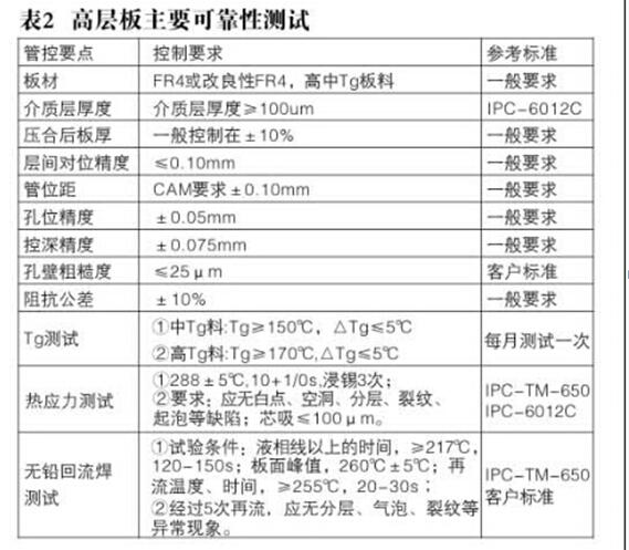
The high-layer plate is generally a system plate, which is thicker, heavier, larger unit size and larger heat capacity than the conventional multi-layer plate. During welding, it needs more heat, and the welding high temperature time is longer. At 217C (melting point of tin-silver-copper solder), it takes 50 to 90 seconds, and the cooling rate of the Multilayer plate is relatively slow, so the reflow testing time is prolonged. Combined with IPC-6012C, IPC-TM-650 standards and industry requirements, the main reliability test of the Multilayer plate.
IV. Conclusion.
For the research literature on the processing technology of Multilayer circuit boards, there are relatively few in the industry. This paper introduces the key process control points of key production processes, such as material selection, laminated structure design, interlayer alignment, inner circuit fabrication, pressing process, drilling process, etc., in order to provide peer reference and understanding. It is hoped that more colleagues will participate in the technical research and exchange of Multilayer circuit boards.
Hello, welcome to visit our official website!
+86 13502814037 (What's up)sales@topscompcbassembly.com

Turnkey Pcba Assembly & Contract Electronic OEM Manufacturing Provider

