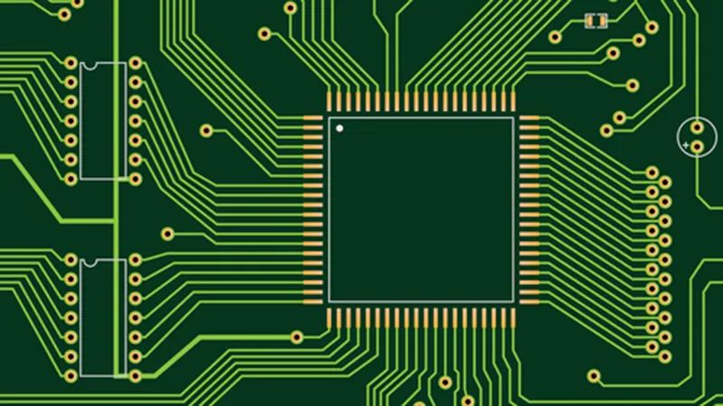
China Topscom provide pcb boards manufacturing and fabrication,Printed Circuit Boards include: PCB Prototype, pcb quick turn,Aluminum PCB, Rigid-Flex PCBs, Metal core PCBs, Flexible PCBs, High Frequency PCBs,High-TG PCBs,Thick-Copper PCBs,HDI PCB,LED PCB,our factory pcb manufacturer experience include:medical devices,automotive electronics, military defense Aerospace,industry,telecom ,led lighting, energy oil gas,related products applications,china Topscom company is a Shenzhen manufacturer, low cheap price,hight quality, It's trustworthy.
Via is an important knowledge point in PCB design, especially for high-speed multi-layer PCB design, via design needs to attract the attention of engineers. Next, let's take a look at the via knowledge in PCB design.
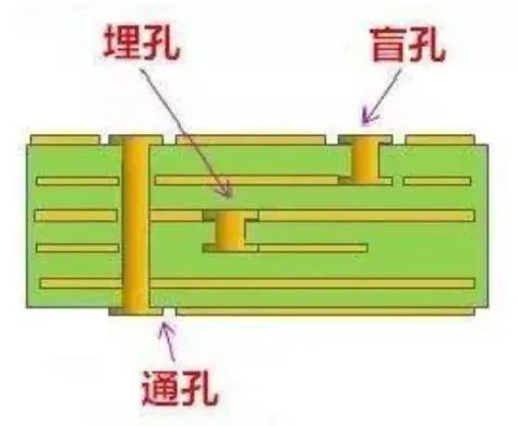
Type of via.
Via are generally divided into three types: via, blind holes and buried holes.
Blind hole: it is located on the top and bottom surfaces of the printed circuit board and has a certain depth, which is used for the connection between the surface circuit and the inner circuit below. the depth of the hole usually does not exceed a certain ratio of the pore diameter.
Buried hole: a connection hole located in the inner layer of a printed circuit board that does not extend to the surface of the circuit board.
Via: this hole passes through the entire circuit board and can be used for internal interconnection or as a positioning hole for the installation of components. Because the via is easier to realize in the process and the cost is lower, the printed circuit board is generally used.
Design rules of via.
In order to integrate design and production, engineers need to consider the following issues:
(1) the via cannot be located on the pad;
(2) the contact area between the metal shell of the device and the PCB extends outward and there can be no via in the 1.5mm area.
(3) there should be no via in the spot coating or printing area of the patch. Such as the use of patch glue dot coating or printing process of CHIP, SOP components under the PCB area.
(4) the inner diameter of the full pass hole requires 0.2mm (8mil) and above in principle, and the outer diameter is above 0.4mm (16mil). If there are difficulties, the outer diameter must be controlled as 0.35mm (14mil).
(5) it is suggested that buried blind holes should not be used in the design of BGA in 0.65mm and above, and the cost will be greatly increased.
(6) the distance between the via and the via should not be too close, drilling is easy to cause hole breakage, generally require hole spacing 0.5mm or above, 0.35mm-0.4mm to avoid, 0.3mm and below prohibited.
Via in ordinary PCB.
In the ordinary PCB design, the parasitic capacitance and parasitic inductance of the via have little influence on the PCB design. For the 1-4 layer PCB design, the 0.36mm/0.61mm/1.02mm (drill hole / pad / POWER isolation zone) is generally selected. Some special signal lines (such as power wire, ground wire, clock wire, etc.) can choose the 0.41mm/0.81mm/1.32mm via, or the other size via can be selected according to the reality.
Via in High Speed PCB.
I. influence.
In high-speed PCB multilayer boards, signals from one interconnect to another interconnect need to be connected through a hole. When the frequency is lower than 1GHz, the via can play a good connection role, and its parasitic capacitance and inductance can be ignored.
When the frequency is higher than 1 GHz, the influence of the parasitic effect of the via on the signal integrity can not be ignored. at this time, the via shows a breakpoint of discontinuous impedance on the transmission path, which will lead to signal integrity problems such as signal reflection, delay, attenuation and so on.
When the signal is transmitted to another layer through the hole, the reference layer of the signal line also acts as the return path of the via signal, and the return current will flow between the reference layers through capacitive coupling, causing problems such as ground elasticity.
It can be seen that in the high-speed PCB design, the seemingly simple via often brings great negative effects to the circuit design. In order to reduce the adverse effects of via parasitic effects, engineers can do as much as possible in the design:
The main results are as follows: (1) choose a reasonable via size. For the multi-layer general density PCB design, the via of 0.25mm/0.51mm/0.91mm (drilling / pad / POWER isolation zone) is better, for some high density PCB, the 0.20mm/0.46mm/0.86mm via can also be used, and for the via of power supply or ground wire, larger size can be considered to reduce the impedance.
(2) the larger the POWER isolation zone, the better. Considering the via density on PCB, it is generally D1 / D2 / 0.41;
(3) the signal routing on PCB should not change layers as much as possible, that is to say, the number of via holes should be reduced as much as possible.
(4) the use of thinner PCB is beneficial to reduce the two parasitic parameters of the via;
(5) the pins of the power supply and the ground should pass through the holes nearby, and the shorter the leads between the holes and the pins, the better, because they will lead to an increase in inductance. At the same time, the leads of the power supply and the ground should be as thick as possible to reduce the impedance.
(6) some grounding holes are placed near the vias of the signal switching layer, so as to provide a short distance circuit for the signal.
Hello, welcome to visit our official website!
+86 13502814037 (What's up)sales@topscompcbassembly.com

Turnkey Pcba Assembly & Contract Electronic OEM Manufacturing Provider

